Lithography Tools
- Double - Side Mask Aligner System
- Direct Writing Maskless Lithography System
- Oven
- Hot Plate
- Fume Hoods
Double - Side Mask Aligner System
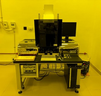
NAME OF INSTRUMENT: DOUBLE - SIDE MASK ALIGNER SYSTEM
COMPANY: OPTICAl ASSOCIATES Inc. (USA)
MODEL NUMBER: 0130-111795 (OAI 806 EBA 500W NUV)
APPLICATIONS: Fabrication of microstructures based on optical lithography process using pre-defined mask with precise alignment on both sides of the wafers. Wafers up to 6” can be used.
Specifications
| Parameter | Specification |
|---|---|
| Mask Rotation | ± 45° |
| Mask Size | Up to 9" × 9" |
| Mask Loading | Vacuum and mechanical clamp |
| Mask/Substrate Pressure | User definable (Electronically Enhanced Hard Contact) |
| Chuck Motion Control | X, Y, Z & Theta (motorized joystick) |
| Exposure Gap | 0–3000 µm |
| Gap Adjustment | 1 µm |
| Mechanical Resolution | 0.1 µm |
| X, Y Travel | ± 5 mm |
| Theta Travel | ± 4° |
| Leveling | Automated wedge-compensation system |
| Overlay Accuracy | Top to back < 2 µm (3σ), Top side to 0.5 µm |
| Substrate Size | Up to 200 mm square |
| Printing Modes | Proximity, Soft, Hard, and Vacuum Contact |
| Printing Resolution |
Vacuum: submicron Hard contact: to 1 µm Soft contact: to 2 µm Proximity: 3–5 µm with 15–20 µm gap |
| Exposure Time | 1–3200 seconds in 0.1 second increments |
| Alignment Optics Magnification |
Top: Continuous zoom – 70× to 400× (optional 140× to 800×) Bottom: 180× |
| Alignment Optics Separation |
Top: 42 mm to outside of mask (optional to 9 mm) Bottom: 19 mm to 200 mm (single microscope: 0 mm to 200 mm) |
Direct Writing Maskless Lithography System
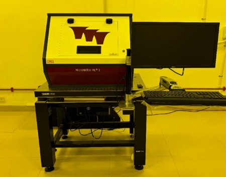
NAME OF INSTRUMENT: DIRECT WRITING MASKLESS LITHOGRAPHY SYSTEM
COMPANY: DURHAM MAGNETO OPTICS LTD (UNITED KINGDOM)
MODEL: MICRO WRITER ML3 PRO WITH DUAL WAVELENGTH LIGHT SOURCE
APPLICATIONS: Maskless Lithography (direct laser writer) to define microstructures based on optical lithography process with a resolution of 0.6 µm.
Specifications
| Parameter | Specification |
|---|---|
| Maximum substrate size | 230 mm × 230 mm × 15 mm |
| Maximum writing area | 195 mm × 195 mm |
| Exposure minimum feature sizes | 0.6 µm, 1 µm, 2 µm, 5 µm. 0.4 µm as option. |
| Surface tracking autofocus system? | Yes |
| Edge locating laser for automatic wafer centering? | Yes |
| Greyscale lithography? | Yes |
| Alignment microscope objectives | x3, x5, x10, x20. x50 as option. |
| Automatic lens changer for exposure resolution and alignment microscope? | Yes |
| Backside alignment? | Available as option |
| Exposure wavelength | 385 nm. 365 nm available as option. |
| Maximum writing speed |
17 mm²/min at 0.6 µm resolution 50 mm²/min at 1 µm resolution 120 mm²/min at 2 µm resolution 180 mm²/min at 5 µm resolution |
| Overlay alignment accuracy at best resolution | ±0.5 µm |
| Minimum addressable grid | 100 nm |
| Motion stage minimum XY step size | 4 nm |
| XY interferometer resolution | 1 nm |
| Optical surface profiler Z resolution | 100 nm |
Oven
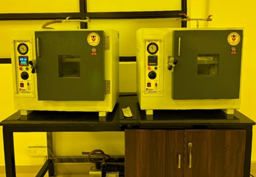
NAME OF INSTRUMENT: VACUUM OVEN
COMPANY: M.K. SCIENTIFIC INSTRUMENTS
APPLICATIONS: Wafer drying, Cleaning via annealing, heat treatment up to 500°C in nitrogen or vacuum environment
Specifications
Hot Plate
Upcoming...
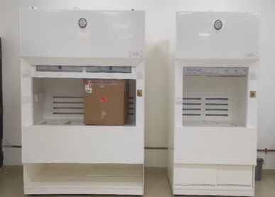
Fume Hoods
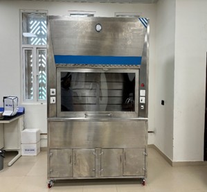
NAME OF INSTRUMENT: ORGANIC WET CHEMICAL BENCH
COMPANY: NANO CLEAN CONTAMINATION CONTROL SOLUTION (INDIA)
APPLICATIONS:For chemical cleaning of the wafers, semiconductor device processing,
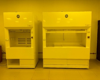
NAME OF INSTRUMENT: ELECTROPLATING WET CHEMICAL BENCH & LAMINAR AIR FLOW BENCH
COMPANY: NANO CLEAN CONTAMINATION CONTROL SOLUTION
NAME OF INSTRUMENT: IN-ORGANIC WET CHEMICAL BENCH & TMAH BENCH
COMPANY: NANO CLEAN CONTAMINATION CONTROL SOLUTION (INDIA)
APPLICATIONS:for chemical cleaning of the wafers, wet chemical etching, acid cleaning, HF treatment, semiconductor device processing,